Hybrid Integrated Circuit Packaging 点击:65 | 回复:0
混合集成电路(HIC)是将裸芯片直接固定在基板上并实现与基板互连而形成的高装配密度电路。
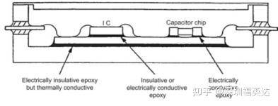
A hybrid integrated circuit (HIC) is a high assembly density circuit formed by directly fixing the bare chip onto the substrate and realizing interconnection with the substrate. HIC can be two or more components packaged together to form microelectronic circuits, such as an integrated circuit and a passive electronic component packaged together and then installed on a PCB. Producing HICs is a relatively simple procedure. The general steps include assembling IC and passive components on the same substrate and then packaging them with plastic and other materials. Assembling components on the same substrate can reduce the number of solder joints and the spacing between components and the current path.

Figure 1. Hybrid integrated circuit.
The HIC can be divided into two categories of thin-film hybrid integrated circuits and thick-film hybrid integrated circuits. The substrate material of thin film HIC can be glass or ceramic, which can bring better heat dissipation performance after soldering. The interconnecting wires and pads prefabricated on the substrate are generally made by vapor deposition or sputtering metal films, then etched with specific patterns by photolithography. Physical vapor deposition usually adopts flash evaporation to deposit metal materials on the substrate. The sputtering method can achieve a high film deposition rate without high-temperature treatment. In addition, the wire width and spacing of thin film hybrid integrated circuits are generally 3 – 5 mils.
Ceramic materials such as aluminum oxide, aluminum nitride, and beryllium oxide are also selected as interconnection substrates for thick film HICs. The difference is that thick film HIC uses screen printing technology to deposit conductive solder, such as solder paste on the substrate to form a thick film. The thick film is required to have good conductivity, compatibility, and adhesion. The wire width and spacing of thick film HICs are very small. Many manufacturers will choose 10-20mils conductors. Compared with thin wires, thicker wires can increase the yield of components. Besides, thick film HICs have better cost advantages than thin film HICs.
Multichip Module (MCM)
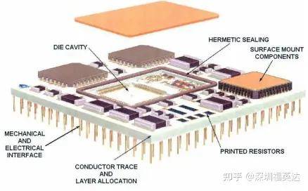
MCM is an extended product of the development of HIC technology. The development of MCM is attributed to the increase of package density by hybrid integration technology, representing that the MCM substrate will contain more IC chips. The classification of MCMs includes MCM-L (laminated), MCM-C (co-fired ceramics), and MCM-D (deposited). MCM substrates can be a rigid-type, flexible-type, and rigid-flexible type. Rigid MCM-L substrates are usually made of epoxy-based polymer resin dielectrics and reinforced with glass fibers. MCM-L packaging technology is one of the lowest densities, and the cost of manufacturing is naturally the lowest. It is worth noting that MCM-L is very similar to chip-on-board technology (COB). MCM-C is developed on the basis of co-fired ceramic HIC technology. There are two firing technologies of ceramic substrates, including high-temperature co-fired ceramic and low-temperature co-fired ceramic.

Figure 2. A multichip module structure.
Shenzhen Fitech provides customers with high-quality ultrafine solder paste products, which can be used as the conductive material for IC packaging. The melting point temperature of SnBiAg solder paste can be as low as 139℃, which is suitable for low-temperature soldering scenarios. Fitech can also provide gold-tin solder paste with a melting point of 280℃ to meet the needs of high-temperature soldering. In addition, there are other types of solder pastes with different temperatures. Welcome to learn more information.
楼主最近还看过

官方公众号

智造工程师
-

 客服
客服

-

 小程序
小程序

-

 公众号
公众号


 工控网智造工程师好文精选
