电镀共晶锡铋焊膏凸点的性能 点击:127 | 回复:0

电子行业对更轻、更小、更灵活的产品的需求不断增长。为了实现芯片的小型化,焊盘间距变得越来越小。此外,为了充分利用芯片空间,越来越多的制造商采用倒装芯片封装技术,可以生产更多的I/O接口、更好的电气性能和更小的封装尺寸。研究人员发现,采用电镀焊膏制作凸块可以满足倒装芯片封装的要求。电镀锡膏工艺可以解决成本和批量生产问题,满足细间距要求。共晶锡铋焊膏适合生产熔点低、机械性能好的微凸块。
The electronics industry has an increasing demand for lighter, smaller, and more flexible products. In order to realize the miniaturization of chips, the pad pitch becomes smaller and smaller. In addition, in order to make full use of chip space, more and more manufacturers adopt flip-chip packaging technology, which can produce more I/O interfaces, better electrical performance, and smaller package size. The researchers found that the use of electroplated solder paste to make bumps can meet the requirements of flip-chip packaging. The electroplating solder paste process can solve cost and mass production problems and meet fine-pitch requirements. Eutectic tin-bismuth solder paste is suitable for producing micro-bumps with low melting points and good mechanical properties.
The flip chip requires placing a metal layer under the bumps. Solder paste is then deposited on the pads and reflowed to form solder joints. The eutectic Sn-Bi solder paste can be electroplated onto the pads using a commercial electroplating DC pulse electroplating apparatus. Roh et al. (2014) conducted experiments on electroplating eutectic SnBi solder paste and tested solder joint reliability. Constant potential and current density are the keys to stable electroplating. Plating at 30 mA/cm2 for 15 minutes resulted in columnar Sn-Bi bumps with an average bump diameter and height of 22 ± 0.4 and 18 ± 06 lm, respectively (Roh et al., 2014).
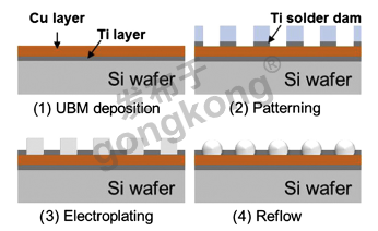
Figure 1. The schematic diagram of electroplated SnBi solder bump process (Roh et al., 2014).
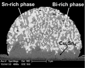
Figure 2. The cross-sectional image of solder bump after 20 minutes of reflow at 170℃ (Roh et al., 2014).
After 20 minutes of reflow at 170°C, the SnBi solder paste wetted the pads and formed hemispherical solder joints. The white part of Figure 2 is the bismuth-rich phase, and the gray section is the tin-rich phase. At the same time, the growth of the intermetallic compound Cu6Sn5 can be observed in the solder joints. The growth of Cu6Sn5 is related to the reflow time. Longer reflow time can result in excessively Cu6Sn5 formation. Other IMCs, such as Cu3Sn, are unlikely to generate during reflow. Generally speaking, Cu3Sn appears gradually in the aging test and increases with the aging time.
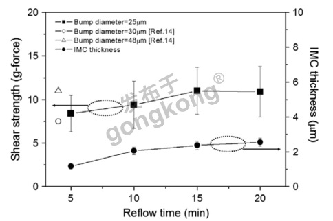
Figure 3. The relationship between reflow time and shear strength (Roh et al., 2014).
As shown in Figure 3, the shear strength of the electroplated eutectic SnBi bumps increases as the reflow time increases. Reflow soldering time should be too long. Otherwise, the solder joints will become brittle and cause fracture due to the overgrowth of the IMCs. Brittle fracture also occurs during thermal aging. With increasing aging time, brittle IMCs grow spontaneously, eventually leading to brittle fracture. At present, many experimental conclusions show that doping nanometal particles can reduce the brittle fracture issue. Eutectic SnBi bumps have low hardness and can be applied to specific components according to actual needs.
Fitech is a manufacturer dedicated to the production of high-reliability solder paste. The products cover various alloy combinations, such as tin-bismuth and tin-silver-copper. Welcome to learn more details.
Reference
Roh, M.H., Jung, J.P., & Kim, W.J. (2014), “Microstructure, shear strength, and nanoindentation property of electroplated Sn–Bi micro-bumps”, Microelectronics Reliability, 54, pp. 265-271.


楼主最近还看过

官方公众号

智造工程师
-

 客服
客服

-

 小程序
小程序

-

 公众号
公众号


 工控网智造工程师好文精选
